更便宜、更小巧的DNA测序设备的研制受到若干因素的限制,其中包括对成像技术的需求。一项新的DNA测序技术不需要用光学方式读取数据,而是通过直接感应由模板引导的DNA合成所产生的氢离子来获取序列数据。该技术提供了一个在大规模并行半导体感应设备上或离子芯片上进行低成本、规模化测序的途径。相关反应都是用天然核苷酸进行的,各个离子敏感性芯片都是一次性的,价格都不高。该系统已用于对三个细菌基因组和一个人基因组进行测序,其中的人基因组是因发现“摩尔定律”而知名的戈登•摩尔的基因组。
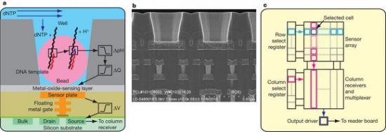
Figure 1: Sensor, well and chip architecture.
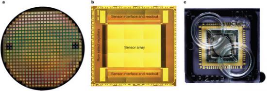
Figure 2: Wafer, die and chip packaging.
生物探索推荐英文摘要:
An integrated semiconductor device enabling non-optical genome sequencing
The seminal importance of DNA sequencing to the life sciences, biotechnology and medicine has driven the search for more scalable and lower-cost solutions. Here we describe a DNA sequencing technology in which scalable, low-cost semiconductor manufacturing techniques are used to make an integrated circuit able to directly perform non-optical DNA sequencing of genomes. Sequence data are obtained by directly sensing the ions produced by template-directed DNA polymerase synthesis using all-natural nucleotides on this massively parallel semiconductor-sensing device or ion chip. The ion chip contains ion-sensitive, field-effect transistor-based sensors in perfect register with 1.2 million wells, which provide confinement and allow parallel, simultaneous detection of independent sequencing reactions. Use of the most widely used technology for constructing integrated circuits, the complementary metal-oxide semiconductor (CMOS) process, allows for low-cost, large-scale production and scaling of the device to higher densities and larger array sizes. We show the performance of the system by sequencing three bacterial genomes, its robustness and scalability by producing ion chips with up to 10 times as many sensors and sequencing a human genome.